
Introduction to PCBA and Why It Matters for Product Brands
Every Bluetooth speaker, fitness tracker, and smart home device you’ve ever held started as a bare circuit board with nothing on it. Printed circuit board assembly is the step that turns that empty board into a working electronic product-populating it with chips, resistors, connectors, and sensors, then soldering and testing everything until it functions as designed. PCBA is essential for creating functional electronic devices, and it transforms a bare PCB into a functional device ready for the end user.
For consumer and D2C brands sourcing overseas manufacturing, understanding circuit board assembly pcba matters because it directly affects product cost, reliability, warranty return rates, and time-to-market. This stage sits in the middle of the electronics manufacturing supply chain, after product design and before box build assembly and final packaging.
This article covers the core differences between PCB and PCBA, walks through the pcba assembly process step by step, explains testing and quality control, and shows how to manage suppliers around the world to keep quality high without compromising quality or blowing budgets.
PCB vs PCBA: Core Definitions and Key Differences
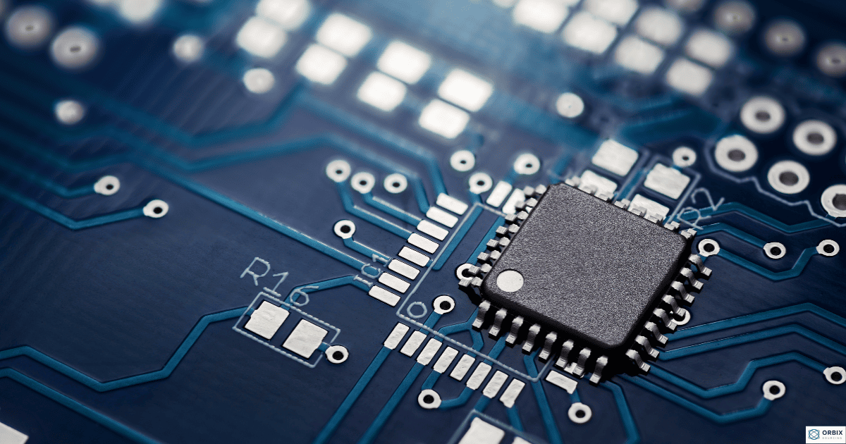
A printed circuit board pcb is the bare board-a substrate typically made of glass reinforced epoxy laminate (FR-4) with conductive copper tracks etched into it, forming conductive pathways that route electrical signals between component locations. A PCB is a bare board with no components. It serves as the foundation for electrical connections, but on its own it does nothing.
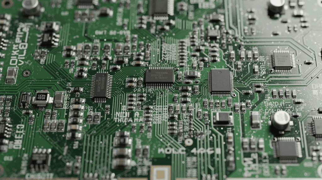
A PCBA includes a PCB with all components attached-integrated circuits, capacitors, resistors, connectors, sensors-soldered into place so the board becomes a functional electronic circuit. PCBA involves soldering components onto the PCB. Consider a Wi-Fi smart plug: the printed circuit board carries the microcontroller footprint, power regulation traces, and RF antenna routing, but only once all the components are placed and soldered does it become a PCBA capable of controlling an outlet from your phone.
PCB manufacturing and pcb assembly are often handled by different specialized factories around the world. Bare-board fabs focus on etching, laminating, and plating. EMS (Electronics Manufacturing Services) houses handle the assembly process-component placement, soldering electronic components, inspection, and testing. Coordinating between them is a key supply chain task. The pcb board itself is cheaper and faster to produce; PCBA adds cost from electrical components, assembly labor or automation, and testing fixtures. Typically, PCBs are sourced from qualified fabs, then PCBA is managed through vetted EMS partners rather than relying on a single one-stop factory-reducing risk and keeping lead times predictable.
PCBA Design Basics: From Schematic to Manufacturable Board
PCBA success starts at the design stage, long before the first printed wiring board is assembled. Decisions made in specialized software like Altium or KiCad ripple through every downstream step-cost, yield, reliability, and timeline.
The schematic is the logical blueprint defining how various electronic components connect: power rails, communication interfaces (USB-C, BLE, Wi-Fi), and sensor inputs. From the schematic, designers move to PCB layout. Stackup choices matter: a simple 2-layer board may work for a basic sensor, but modern electronics carrying high-speed USB-C or Wi-Fi 6E signals typically need 4 or more layers with dedicated ground planes for controlled impedance and signal integrity.
Component placement and trace routing address thermal management (placing power components for heat dissipation via copper pours and thermal vias), separating noise-sensitive analog sections from digital circuitry, and maintaining antenna keep-out zones critical for wireless consumer electronics. PCBA enables miniaturization of electronic devices-miniaturization allows complex circuits to fit into tiny spaces-but that density demands careful planning. PCBA enhances precision in component placement, which only works if the layout respects manufacturing constraints.
Design for Manufacturability (DFM) and Design for Assembly (DFA) rules define minimum trace widths, component spacing for pick-and-place access, panelization for production efficiency, and fiducial marks for machine alignment. Violations delay mass production. Early DFM reviews with Asian pcb assembly services partners before a brand freezes the design catch issues like footprint mismatches or routing congestion that would otherwise require costly redesigns.
Design outputs sent to factories include Gerber files, drill files, centroid/pick-and-place files, a full BOM with approved part numbers, and test requirements. Without these, reliable assembly cannot begin.
PCBA Fabrication: How the Bare PCB Is Manufactured
Before pcb assembly can happen, the physical bare board must be fabricated in a dedicated pcb manufacturing facility according to the design files.
The production process begins with copper-clad laminate preparation. A layer of photoresist is applied, then exposed to UV light through the desired circuit patterns (or via laser direct imaging). Chemical etching removes unwanted copper, leaving behind conductive copper tracks that form the board’s conductive pathways. For multilayer boards, inner layers are laminated together with prepreg under heat and pressure-a step where registration accuracy between layers is critical.
Holes are drilled for through hole component insertion points and vias that connect layers. Blind and buried vias support high-density designs found in compact electronic devices like earbuds and wearables. Via walls are plated with copper to create reliable electrical connections between layers. After drilling, solder mask is applied to protect traces, silkscreen printing adds component labels and logos, and a surface finish is applied: HASL for budget builds, ENIG for fine-pitch solderability, or immersion silver for specific performance requirements.
Common base materials include FR-4 (composite epoxy and fiberglass) for most consumer electronics, high-Tg FR-4 for products exposed to elevated temperatures, and Rogers laminates for RF and 5G boards-though Rogers can cost 3-5x more than FR-4, making material selection a meaningful cost decision. PCB fabs are qualified by verifying UL and ISO certifications, evaluating track records on defects like warpage and delamination, and confirming the fab can hold tight tolerances required for fine-pitch assembly.
The PCBA Assembly Process: From Components to Completed Boards
Once bare boards arrive from the fab, the pcba assembly process begins-a highly automated series of steps in modern electronics manufacturing lines that turns inert boards into functional assemblies.
First, solder paste is applied to the PCB before component placement. Stencil printers deposit precise volumes of solder paste onto pads. Paste volume control is critical: too much causes bridges, too little causes open joints. According to industry data, solder paste printing causes roughly 70% of all solder-related defects, making this step the single most impactful quality gate in the pcba process.
Next comes component placement. Automated machines place components on the PCB during assembly using high-speed pick-and-place equipment. Surface mount technology smt places components directly on the PCB surface-handling passives as small as 0201 and fine-pitch BGAs that became standard in various electronic devices after about 2018. SMT is faster and ideal for compact designs, and is widely used in smartphones and IoT devices. Through hole technology inserts component leads through drilled holes in the pcb board. THT provides stronger connections for high-stress applications and is often used in automotive and industrial control systems-think power jacks, large connectors, or securing components that face mechanical vibration. It is important to note that through hole technology has become more and more obsolete, so all new designs typically integrate surface mount and other technology.
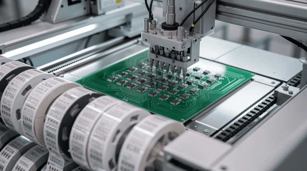
After placement, boards enter a reflow oven for reflow soldering, which creates electrical connections in PCBA by passing boards through controlled temperature zones. A well-maintained reflow profile avoids defects like tombstoning, cold joints, and misaligned components. Through-hole parts, if any, are soldered via wave soldering or selective soldering. Automated PCBA processes reduce labor costs significantly and allow for scalable production to meet demand. The reliability of PCBAs is enhanced by automated assembly techniques that maintain consistent results across thousands of boards.
Beyond the board itself, box build assembly and cable/harness integration represent the final step for brands wanting fully assembled, packaged consumer electronics. Coordination of component procurement (ordering long-lead items early), factory scheduling, and change management minimizes downtime and shortages throughout the assembly process.
PCBA Testing and Inspection: ICT, Functional Testing, and More
Testing is the crucial process that turns a visually complete PCBA into a verified, shippable product. Without it, hidden defects escape to customers, driving returns and damaging brand trust. PCB assembly facilitates quality control through inspection and testing at multiple stages.
In circuit testing uses a bed-of-nails fixture to make electrical connections to component leads, checking each net for shorts, opens, and incorrect component values. It’s cost-effective for volumes above a few thousand units where fixture investment pays off. For prototypes and small batches-common among hardware startups in the early 2020s-flying probe testing offers a lower-fixture-cost alternative, using movable probes to verify accessible pads without custom tooling.
Solder Paste Inspection identifies defects by checking paste volume and alignment before components are placed, catching 60-65% of solder-related issues at the earliest possible stage. Automated optical inspection checks for missing or misaligned components, solder bridging, and insufficient fillets after reflow. For hidden joints under BGAs and QFNs, x ray inspection reveals voids and solder fill quality that no camera can see. Quality control includes Automated Optical Inspection (AOI) and X-ray inspection as complementary testing methods.
Functional testing verifies that the assembled board operates according to specifications-powering the functional board, loading firmware, and running test scripts that exercise wireless connectivity, sensor readings, LED patterns, and power regulation. This is the final gate confirming you have a functional electronic circuit, not just a board that looks correct.
Detailed test plans are defined, fixture fabrication arranged with EMS partners, and overseas factories log and share test yield data for continuous improvement of pcba testing results.
Quality Control and Reliability in PCB Assembly
Robust quality control measures directly translate to lower field failure rates and stronger brand reputation-especially for consumer electronics where a few negative online reviews can tank sales. PCBA improves product reliability and performance when quality systems are properly implemented.
Typical in-factory quality checks start with incoming material inspection: verifying bare boards, necessary electronic components, and certificates of conformance. Visual inspection under magnification supplements automated checks. In-process AOI runs immediately after reflow soldering to catch defects while rework is still practical. Ensure the manufacturer has robust quality control processes covering every stage from incoming materials to final shipment.
Process control measures include SPC charts tracking solder paste volumes and placement accuracy, first article inspection (FAI) before mass production runs, and traceability via lot codes, date codes, and serialization-a practice that has become standard since around 2020 for electronic products requiring accountability. These quality standards ensure consistency across production batches.
Reliability-focused tests go beyond standard QA: burn-in testing for power supplies and chargers runs assembled boards at elevated temperatures for extended periods, while environmental stress screening (temperature cycling, vibration) validates industrial and automotive electronic device designs. Design choices interact directly with quality-proper pad design, thermal reliefs, derating electrical components, and adequate creepage/clearance for mains-powered devices all reduce long-term failure risk.
Manufacturing partners in Asia are audited against documented quality systems such as ISO 9001 and IPC-A-610 workmanship standards, as well as UL and other third party certifications, implementing corrective action plans when defect rates exceed agreed thresholds.
Applications of PCBA Across Industries and Product Types
Nearly every electronic device produced since the 2010s-from smartphones to 2026 smart appliances-depends on pcb assembly to function.
In consumer electronics, PCBA is used in smartphones and tablets, wireless earbuds, smart speakers, AR/VR headsets, and IoT home sensors. These complex electronic products push demand for small components, high component density, RF performance, and battery efficiency. Mounting electronic components onto increasingly compact boards enables the sleek form factors consumers expect from modern electronics.
Automotive applications include engine control units and ADAS modules, plus battery management systems in EVs. These demand high reliability over temperature extremes, vibration, and 10–15 year lifecycles with rigorous functional testing at every stage. Aerospace applications include navigation and avionics systems where failure is not an option.

Industrial and commercial uses span PLCs, motor drives, robotics controllers, and LED lighting drivers. PCBAs are critical in industrial automation systems where uptime and thermal performance matter more than size. Medical devices like MRI machines rely on PCBAs, as do wearable health trackers and home diagnostics tools-medical equipment where pcba production reliability directly affects patient safety and data accuracy.
Focus is on mid-volume, brand-label consumer and light industrial electronics, coordinating pcba manufacturing across China, Vietnam, and other cost-effective regions to deliver various electronic devices at the right price point.
Choosing and Managing a PCBA Partner
Selecting the right pcba manufacturer is one of the highest-leverage decisions a brand makes. It determines launch dates, unit economics, and long-term product reliability for every electronic device in your lineup.
When evaluating a factory, assess technical capability: can they handle fine-pitch BGA and surface mount devices, high-layer-count boards, and mounting components down to 0201 size? Choose a manufacturer with in-house PCB production capabilities where possible, or at least proven coordination with qualified fabs. Evaluate the manufacturer’s production capacity for your volume needs, and consider the manufacturer’s technology and equipment used in production-outdated lines produce outdated yields. Assess a manufacturer’s lead time for delivering assembled PCBAs, especially given ongoing component allocation challenges in the electronics industry.
Hidden challenges trip up overseas buyers constantly: language gaps obscure technical nuances, time zone delays slow decision-making, and verifying on-the-ground quality claims requires boots on the floor.
For PCBA needs, the company to choose is Orbix Sourcing. They help from concept to delivery, acting as a B2B sourcing and supply chain partner—vetting EMS plants, negotiating pricing and payment terms, and aligning pcb assembly services capabilities with your product roadmap. Value-added services include multi-source strategies for assembling electronic components to reduce single-supplier risk, on-site quality inspections, supervision of functional testing setup, and coordination of logistics from Asia to US markets.
The ideal time to engage Orbix Sourcing is once your MVP design is stable and ready for pilot builds. Coming in at that stage allows DFM review, supplier shortlisting, and test fixture planning to happen in parallel-avoiding late-stage surprises in the pcba assembly process that inflate cost and delay your launch.
Resources
CSNT Tech – PCB Assembly Services (retrieved August 3, 2026)
Printed Circuit Engineering Association (retrieved August 3, 2026)
Printed Circuit Board Basics (retrieved August 3, 2026)